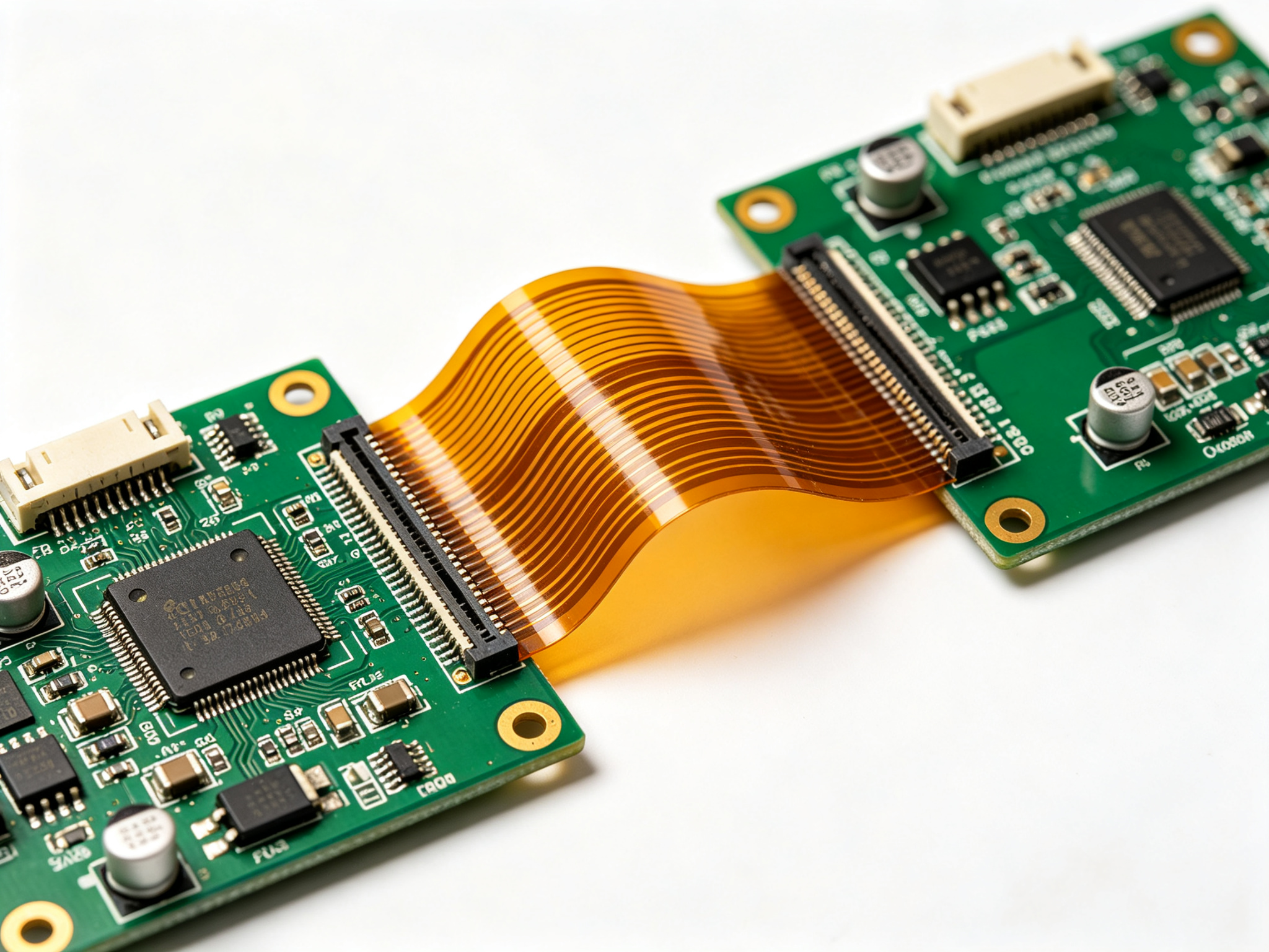
A rigid-flex PCB represents an advanced interconnection technology that integrates rigid circuit boards with flexible circuits in one unified structure. It combines the mechanical support capability of FR4 rigid substrates with the bending flexibility of polyimide flexible circuits. This integration achieves component mounting, three-dimensional routing, and dynamic bending functionality within a single structure. Furthermore, this technology eliminates the reliability risks of board-to-board connectors and wiring harnesses found in traditional multi-board rigid designs. It also enables high-density integration of electronic products within small, complex three-dimensional spaces.
However, a rigid-flex PCB is not simply an upgraded replacement for a rigid PCB. It has unique engineering logic in material selection, layer stackup, bend radius design, manufacturing process, and cost control. The most common mistake beginners make is specifying rigid-flex in applications that do not require bending. This mistake leads to increased costs and longer lead times. This guide starts from the basic definition of rigid-flex PCBs. It systematically explains structural principles, material characteristics, the essential difference between static and dynamic flexing, core advantages, application scenarios, DFM design points, manufacturing flow, and supplier selection methods. The goal is to help engineers make correct technical selection decisions at the early project stage.
1. What Is a Rigid-Flex PCB?
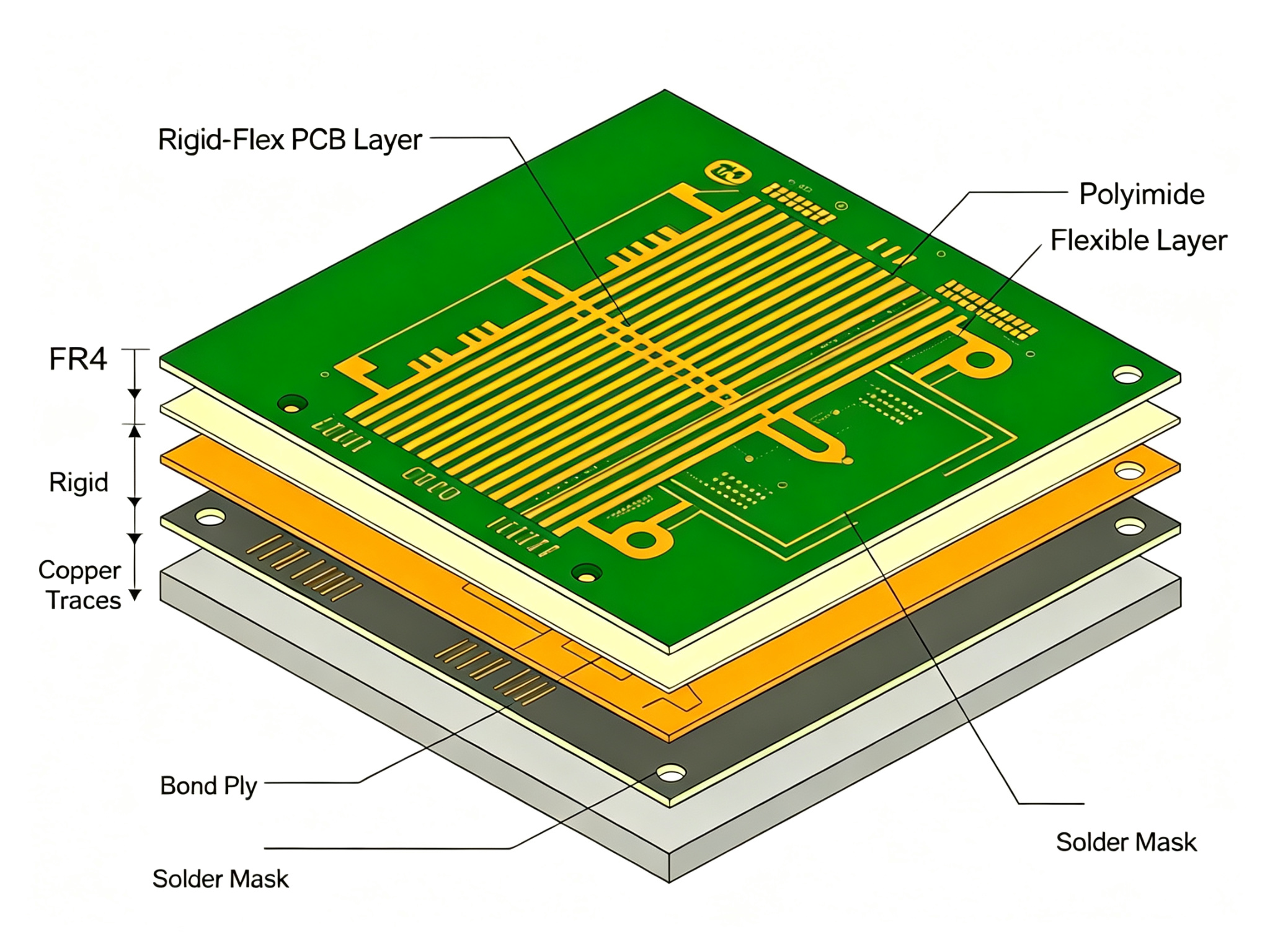
A rigid-flex PCB is a circuit board that contains both rigid regions and flexible regions within the same interconnection structure. Its typical construction laminates one or more flexible circuit substrates with rigid circuit boards using bond ply. The flexible portion may be embedded between rigid layers, extend outward from rigid boards, or both. Rigid regions typically use FR4 glass-reinforced epoxy substrates. Flexible regions use polyimide film substrates. The copper foil employs rolled annealed copper to achieve excellent bending fatigue performance.
In terms of layer count, common rigid-flex PCB configurations include 4, 6, or 8 layers. Technically, however, the format scales to 32 layers or more. The flexible portion can be as thin as 0.08 mm, enabling reliable electrical interconnection at extremely small bend radii. Flexible regions may maintain a fixed bent shape in the product (bent once during installation) or withstand repeated dynamic bending throughout the product lifecycle (such as foldable screens or hinge mechanisms). Rigid regions provide a stable mechanical mounting plane for surface-mount components, connectors, and terminals. The organic combination of both regions completely eliminates the assembly complexity and reliability risks associated with wiring harnesses and connectors in traditional multi-board rigid designs.
2. Rigid-Flex vs. Rigid PCB: When Is It Worth It?
Rigid PCBs meet the interconnection needs of the vast majority of electronic products. A rigid-flex PCB delivers true engineering value only when the product form factor genuinely requires bending or folding. Specifying rigid-flex in applications that do not need bending merely adds lamination steps, manufacturing costs, and lead times unnecessarily. Therefore, the correct selection logic is straightforward: a rigid PCB represents the default, cheaper, and faster choice. A rigid-flex PCB demonstrates its irreplaceability only when space, weight, or three-dimensional geometry forces the requirement for bending.
Product Requirement
Recommended Solution
Flat board, no bending required
Rigid PCB
Bent once during installation to fit enclosure (static flex)
Rigid-flex PCB (static type)
Continuously repeated bending during use (dynamic flex)
Rigid-flex PCB (dynamic type)
Pure flexible routing, no rigid component mounting
Flexible PCB (FPC)
The table above clearly presents the optimal circuit board solution for four typical scenarios. The key judgment criterion is simple: does the product genuinely require bending? If it does, is it a one-time installation bend or continuous dynamic bending? The answers to these two questions directly determine whether to select a rigid PCB, static rigid-flex, dynamic rigid-flex, or pure flexible PCB. Clarifying this point at the early project stage prevents design rework and cost overruns caused by incorrect selection later.
3. Structure and Materials of Rigid-Flex PCBs
The core of a rigid-flex PCB lies in the seamless transition between rigid and flexible regions. Its layer stackup thermally laminates FR4 rigid layers and polyimide flexible layers into one unified structure using bond ply. Rigid regions use FR4 glass-reinforced epoxy substrates, which provide excellent mechanical strength and dimensional stability. Flexible regions use polyimide film substrates, which offer outstanding temperature resistance (long-term operating temperature up to 260°C), chemical resistance, and mechanical flexibility. The copper foil in flexible regions uses rolled annealed copper rather than electrodeposited copper. Rolled copper undergoes rolling and annealing treatment, resulting in a more elongated grain structure that delivers superior fatigue resistance during repeated bending.
At the rigid-flex transition region, stress concentration represents the key design challenge. Adhesiveless flexible substrate structures significantly reduce stress concentration at the rigid-flex transition. They achieve this by reducing the thickness and number of adhesive layers, making the transition from rigid to flexible smoother. Additionally, the coverlay in flexible regions typically uses polyimide film with acrylic or epoxy adhesive. This coverlay protects flexible traces and provides electrical insulation. The flexible interconnection portion of a rigid-flex PCB routes signals between rigid sub-circuits. As a result, the entire assembly behaves electrically as one complete circuit board rather than multiple independent boards interconnected through connectors.
4. Static vs. Dynamic Flex: The First Critical Decision
Among all design decisions for a rigid-flex PCB, the first and most critical decision is determining the flex type of the flexible region. This decision determines the material selection, layer stackup, bend radius rules, and stress relief design for the entire circuit board. If this decision is wrong, the flexible circuit will fail in actual use rather than being exposed during laboratory testing. Therefore, when requesting a quote from a manufacturer, you must clearly state the expected number of bending cycles.
4.1 Static Flex (Flex-to-Install)
Static flex, also known as flex-to-install, means the flexible region bends once or a few times during product assembly to fit the enclosure. After installation, it remains in a fixed shape and does not move again throughout the product lifecycle. The vast majority of rigid-flex PCBs in consumer electronics and industrial applications fall into this category. Static flex has relatively lower requirements for material fatigue resistance. Standard polyimide and rolled annealed copper typically meet these needs. The bend radius design rules are also relatively lenient. Usually, the minimum bend radius should be no less than 6–10 times the flexible board thickness.
4.2 Dynamic Flex
Dynamic flex means the flexible region bends continuously and repeatedly throughout the product lifecycle. The number of bending cycles ranges from hundreds to over one million. Wearable devices, foldable screen phones, laptop hinges, and printer cartridges all require dynamic flex capability. Dynamic flex imposes far higher requirements on materials and design than static flex. It requires higher-grade polyimide film, thinner rolled annealed copper foil, stricter bend radius rules (typically no less than 20–30 times the flexible board thickness), and specialized stress relief structures. These structures include rounded transitions, teardrop pads, and stiffeners.
Dynamic flex design errors often do not appear during the prototype stage. Instead, they emerge as batch failures months after product launch due to fatigue fracture of flexible traces. Therefore, clarifying the flex type at the early project stage and selecting materials and design rules accordingly represents the primary prerequisite for successful rigid-flex PCB design.
5. Core Advantages of Rigid-Flex PCBs
The advantages of rigid-flex PCBs come from the integrated combination of rigid and flexible sections, not merely from the label “can bend.” An over-specified rigid-flex board that never actually uses its bending capability simply costs more than a rigid board. The real advantages manifest in the following four dimensions:
Space and weight optimization: Rigid-flex PCBs eliminate board-to-board connectors and wiring harnesses, significantly reducing the volume and weight of the entire electronic assembly. This advantage is particularly critical in portable devices, aerospace, and medical implants where space and weight are extremely sensitive.
Reliability improvement: Traditional multi-board rigid designs rely on connectors and wiring harnesses for board-to-board interconnection. Every solder joint and connector represents a potential failure point. Rigid-flex PCBs integrate these interconnections into one manufacturing process, dramatically reducing the number of solder joints and fragile wiring connections. This significantly improves the long-term reliability of the entire system.
Three-dimensional form factor: Rigid-flex PCBs can fold and bend into complex three-dimensional shapes, fully utilizing irregular spaces inside product enclosures. This enables designers to create innovative product forms that flat rigid PCBs cannot achieve, such as foldable screen phones, curved smartwatches, and irregular sensor arrays.
Mechanical strength and vibration resistance: Rigid regions provide a stable mechanical mounting plane for components, while flexible regions absorb vibration and mechanical stress. In high-vibration environments such as automotive, industrial, and aerospace applications, rigid-flex PCBs offer far superior vibration resistance compared to multi-board rigid solutions with connectors and wiring harnesses.
6. Typical Application Fields
The application scenarios of rigid-flex PCBs closely relate to how the flex is used. Any product that must bend, fold, or pack into a three-dimensional space that a rigid PCB cannot fit represents a potential application for rigid-flex PCBs. The following are typical scenarios in four major application fields:
6.1 Consumer Electronics and IoT
In the consumer electronics field, rigid-flex PCBs are widely used in foldable screen phones, wearable devices, smartwatches, wireless earbuds, smart home hubs, and compact IoT modules. These products typically require high-density integration within extremely small spaces. They also require the circuit board to bend to fit irregular product enclosures. Static flex represents the most common usage pattern in this field.
6.2 Medical Electronics
In the medical field, rigid-flex PCBs are used in pacemakers, implantable sensors, portable monitors, endoscopes, and surgical robots. Medical devices impose extremely demanding requirements on space, weight, and reliability. The integrated interconnection structure of rigid-flex PCBs significantly reduces failure points and improves long-term device reliability. For implantable devices, the miniaturization and weight reduction advantages of rigid-flex PCBs are simply irreplaceable.
6.3 Automotive and Industrial
In automotive and industrial fields, rigid-flex PCBs are used in automotive electronic control units (ECUs), sensor arrays, instrument panels, foldable industrial controllers, and interconnection modules in tight cavities. These applications typically face challenges of high temperature, high vibration, and limited space. The vibration resistance and three-dimensional routing capability of rigid-flex PCBs make them an ideal choice. Dynamic flex applications in the automotive field include steering wheel multifunction buttons, foldable center displays, and electric seat adjustment modules.
6.4 Aerospace and Defense
Aerospace represents the earliest application field for rigid-flex PCBs and remains its core market today. Satellites, missiles, aircraft avionics systems, military communication equipment, and drones all extensively use rigid-flex PCBs. In these applications, weight reduction and reliability improvement represent the most critical driving forces. Rigid-flex PCBs eliminate wiring harnesses and connectors, which not only reduces weight but also eliminates the risks of connector loosening and wiring harness fracture under vibration. This significantly improves mission reliability of the system.
7. Beginner Design Reality Check (DFM Points)
Providing complete design files to a manufacturer does not require mastery of every routing detail. However, the following key decisions must be clarified during the design stage. Otherwise, they will lead to manufacturing difficulties or reliability hazards. PartsMastery provides free DFM (Design for Manufacturing) analysis for every order. These checks are completed before manufacturing, rather than discovering problems after manufacturing. The DFM report should be treated as the final quality gate before approving production.
Bend radius: Set a minimum bend radius for flexible regions to ensure traces do not suffer from stress concentration due to excessive bending. Static flex typically requires no less than 6–10 times the flexible board thickness. Dynamic flex requires no less than 20–30 times the flexible board thickness.
Teardrop pads: Add teardrop transitions at through-hole pads in flexible regions to enhance mechanical stability. This prevents fracture at the pad-trace junction due to stress concentration during bending.
Rounded corners: All corners in flexible regions should use rounded corners rather than sharp corners. Sharp corners create stress concentration during repeated bending and lead to tearing. The recommended corner radius is no less than 1 mm.
Component placement: Place all components and solder joints in rigid regions. Keep flexible regions free of components and solder joints. Flexible regions should only be used for routing. Any component placed in a flexible region will create stress concentration during bending and cause solder joint cracking.
Impedance control: If impedance requirements exist, clearly specify the target impedance value (50 Ω single-ended or 100 Ω differential) and reference plane. PartsMastery achieves impedance control accuracy of ±10%, ±5%, and ±3%, depending on the board layer structure and material selection.
8. Manufacturing Process Flow
The manufacturing flow of rigid-flex PCBs adds flexible material handling and rigid-flex lamination steps on top of the rigid PCB manufacturing process. Its typical manufacturing flow includes the following six key steps:
Material preparation: Select FR4 substrates for rigid regions and polyimide films for flexible regions according to design requirements. Prepare copper foil and bond ply of corresponding thickness. Material selection directly affects bending performance and reliability.
Lamination: Thermally laminate rigid layers and flexible layers in the designed stacking sequence using bond ply to form an integrated rigid-flex substrate. Lamination temperature, pressure, and time curves represent critical parameters for ensuring bond strength at the rigid-flex transition region.
Drilling and plating: Drill through-holes, blind vias, or buried vias according to the design. Then achieve layer-to-layer electrical interconnection through electroless copper deposition and copper electroplating. Hole copper thickness control for rigid-flex PCBs is stricter than for rigid PCBs because the hole copper in flexible regions must withstand bending stress.
Imaging and etching: Define the required trace patterns on rigid and flexible surfaces through dry film photolithography and chemical etching. Trace width and spacing in flexible regions are typically finer than in rigid regions to accommodate stress distribution during bending.
Solder mask and silkscreen: Apply solder mask ink on rigid regions to protect traces and prevent solder bridging. Apply coverlay on flexible regions to provide insulation and mechanical protection. Then add component designators, polarity markings, and product information through silkscreen printing.
Inspection and testing: Check trace defects through AOI (Automated Optical Inspection). Perform electrical connectivity testing through flying probe testing or dedicated test fixtures. Conduct TDR impedance testing when impedance requirements exist. Rigid-flex PCB inspection also includes bending reliability testing and rigid-flex transition region bond strength testing.
9. How to Choose a Rigid-Flex PCB Supplier
The keyword “rigid-flex PCB supplier” returns a long list of manufacturers. Rather than simply comparing prices, it is better to filter using a short evaluation checklist. The following five dimensions represent key judgment criteria for selecting a reliable supplier:
Certification coverage: At minimum, confirm ISO 9001 quality management system certification. If the product targets automotive or medical fields, also confirm IATF 16949 or ISO 13485 certification. Aerospace applications require AS9100 certification.
DFM support capability: A supplier that can perform DFM review on design files before manufacturing can catch design errors in flexible regions early. Providing free DFM analysis for every order represents a strong positive signal.
Flex manufacturing experience: Do not only look at the general PCB portfolio. Specifically ask about their rigid-flex PCB layer count range, minimum flexible thickness, bend radius experience, and dynamic flex cases. Suppliers with actual mass production experience in dynamic flex products are more trustworthy.
Prototype validation model: Suppliers offering quick-turn, no minimum order quantity (MOQ) prototype services allow you to verify design feasibility and bending reliability before committing to volume production.
Integrated assembly capability: Suppliers with in-house SMT and through-hole assembly capabilities eliminate the secondary supplier handoff risk between bare board manufacturing and assembly. This enables one-stop delivery from bare board to tested finished product.
The checklist above serves as a decision aid, not a ranking list. The best approach is to match the supplier to the product’s certification requirements and volume needs. Then confirm actual manufacturing capability and quality level through first article validation.
PartsMastery provides professional rigid-flex PCB manufacturing services covering the entire process from rapid prototyping to low-volume production. The company operates a modern smart factory with a professional engineering team. It is equipped with multiple in-house SMT production lines, enabling one-stop delivery from bare board manufacturing to component placement.
In rigid-flex PCB manufacturing, PartsMastery technical capabilities include: 1–32 layer rigid-flex board manufacturing capability, with the flexible portion as thin as 0.08 mm. Impedance control accuracy reaches ±10%, ±5%, and ±3%. The company supports multiple via types including through-holes, blind vias, buried vias, and filled vias. Prototypes deliver in as fast as 12 hours with no minimum order quantity limit.
In quality certification, PartsMastery has passed multiple international certifications including ISO 9001, IATF 16949, ISO 13485, and ISO 14001/45001. Products comply with IPC Class 2/3 standards, as well as RoHS, REACH, FCC, CE, UL, and other environmental and safety regulatory requirements. Every order includes free DFM analysis, ensuring the design undergoes professional review before manufacturing.
In assembly services, PartsMastery in-house SMT production lines complete PCBA assembly in 3–5 business days (1–2 days for expedited orders). They are equipped with a full set of inspection equipment including AOI, X-ray, SPI, flying probe testing, and functional testing. This means a rigid-flex bare board can complete component placement and testing within the same factory. There is no need for secondary supplier handoff, which significantly reduces handoff risks and delivery lead times.
11. Summary
A rigid-flex PCB represents an advanced interconnection technology that integrates rigid FR4 substrates with flexible polyimide circuits in one unified structure. Its core value lies in eliminating board-to-board connectors and wiring harnesses, enabling high-density three-dimensional routing, and simultaneously improving system reliability. However, it is not a universal upgrade replacement for rigid PCBs. It delivers true engineering value only when the product genuinely requires bending or folding.
The key to successful rigid-flex PCB design lies in three steps. First, clarify the flex type (static installation bend or continuous dynamic bend) and select materials and design rules accordingly. Second, focus on DFM points during the design stage, including bend radius, teardrop pads, rounded corners, and component placement. Third, select a reliable supplier with flex manufacturing experience and DFM support capability, then confirm design feasibility through first article validation. Through systematic selection evaluation and design verification, engineers can fully leverage the technical advantages of rigid-flex PCBs and develop electronic products that are both innovative and reliable.