




In electronic hardware development, calculating the full cost of printed circuit board (PCB) production has long been a complex challenge for project budgeting. From bare board fabrication to final assembly, various hidden costs often exceed initial estimates, leaving hardware engineers and New Product Introduction (NPI) procurement managers wondering: what is the real cost of a custom PCB?
In reality, the cost of a custom PCB is not a fixed static figure, but a dynamic calculation covering the entire chain of bare board manufacturing, global component sourcing, and finished product assembly. Adopting a fragmented supply chain model — working with separate vendors for bare boards, sourcing components through middlemen, and outsourcing structural parts to third-party factories — will significantly drive up the Total Cost of Ownership (TCO) of the project.
This article breaks down the core components of PCB pricing in detail, shares actionable cost optimization methods aligned with manufacturing process logic, and explains how to achieve dual optimization of project cost and delivery efficiency while meeting international quality standards through an integrated end-to-end ODM/NPI manufacturing service provider.

1. Five Core Factors Driving Bare PCB Manufacturing Costs
Bare board production is the foundational component of overall PCB costs. Understanding how different engineering parameters and process tolerances impact costs helps R&D teams control production expenses from the source through Design for Manufacturing (DFM).
| Cost Driver | Impact on Pricing | Cost Optimization Tips |
|---|---|---|
| Layer count & board size | 高 | Optimize routing to reduce layer count (e.g., from 6 layers to 4 layers), minimize overall board dimensions, and improve material utilization per panel |
| Substrate material selection | 中-高 | Use standard FR-4 for general consumer electronics; upgrade to high-Tg, halogen-free, or polyimide materials only for high-temperature or high-frequency requirements |
| Via technology | 高 | Prioritize standard through-hole vias; blind vias, buried vias, and microvias require multiple lamination cycles and significantly increase production costs |
| 表面处理 | 中型 | Lead-free HASL offers the best cost performance; use ENIG or immersion silver only for fine-pitch BGA or high-reliability applications |
| Impedance control | 中型 | Apply impedance control only to critical high-speed signal traces; full-board impedance control requires strict dielectric testing and adds extra production costs |
1.1 Layer Count and Board Dimensions
The number of layers and physical size of a circuit board directly determine the consumption of raw materials such as fiberglass and copper foil. Conventional double-sided boards benefit from mature processes and low material waste, making them the most cost-effective option. For 4-layer, 8-layer, and higher-tier HDI boards, costs increase exponentially with the number of layers.
Each additional layer imposes stricter requirements for interlayer alignment accuracy, lamination process time, and quality inspection standards. The added production steps and labor hours directly increase bare board manufacturing costs.
1.2 Substrate Material Selection
Standard FR-4 substrate delivers excellent cost efficiency and meets the performance needs of most consumer electronic products. If the product must operate in extreme temperature environments or carry high-frequency RF and high-speed signal transmission, it is necessary to upgrade to specialized substrates such as high-Tg FR-4, PTFE, polyimide (for rigid-flex boards), or metal-core (aluminum/copper base) materials.
These high-end specialty substrates have much higher procurement costs than standard FR-4, with some high-frequency materials costing several times more than conventional FR-4.
1.3 Surface Finish Processes
The core function of surface finish is to protect exposed copper layers from oxidation and corrosion, while providing a flat and reliable contact surface for component soldering. Lead-free Hot Air Solder Leveling (HASL) is the mainstream process for low-budget projects, with mature technology and affordable pricing.
However, if the board carries fine-pitch components such as BGA or QFP, the insufficient flatness of HASL surfaces can easily cause soldering defects such as cold joints and bridging. In this case, it is necessary to upgrade to Electroless Nickel Immersion Gold (ENIG) or OSP processes to ensure pad flatness and soldering reliability, which correspondingly increases upfront manufacturing costs.
1.4 Via and Drilling Complexity
Every drill hole on a circuit board consumes equipment runtime and causes tool wear. Standard mechanically drilled through-holes have mature processes and low unit costs. However, high-density interconnect (HDI) designs requiring laser-drilled microvias, blind vias, or buried vias require the board to go through multiple lamination and drilling cycles, doubling the production workflow.
Advanced via technologies not only increase material and labor costs but also reduce production yield, often doubling overall manufacturing expenses.
1.5 Impedance Control Requirements
Impedance control is a necessary requirement for high-frequency and high-speed signal transmission, but mandatory full-board impedance control will significantly increase production costs. Impedance control requires strict management of dielectric layer thickness, copper trace width, and dielectric constant, and additional dielectric testing steps are needed during production, placing higher demands on process stability.
Applying impedance control only to critical signal traces can effectively control cost increments while ensuring performance.
2. PCB Assembly and Component Sourcing: Overlooked Cost Variables
Many teams only focus on bare board quotes when calculating PCB costs, but overlook the proportion of assembly and component sourcing expenses. In fact, bare board costs account for a limited share of total PCB costs. Differences in component selection, sourcing, and assembly processes are the core variables that affect the final total cost.

2.1 Turnkey Procurement vs. Consignment Procurement
Many companies choose to source components independently (consignment model), believing it can reduce material costs. In practice, however, this often leads to cumbersome process management, high logistics costs, and low material kitting rates, and even carries the quality risk of purchasing counterfeit components from informal channels.
The turnkey procurement model, where the manufacturing service provider handles the full-process procurement of the complete Bill of Materials (BOM), leverages economies of scale to obtain better material pricing. Backed by a global supply chain layout, PartsMastery guarantees 100% authentic sources for all components, paired with strict incoming quality control systems and stable delivery cycles, ultimately helping customers reduce the comprehensive cost per unit product.
2.2 Cost Differences Between SMT and THT Assembly
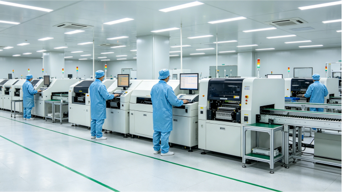
Surface Mount Technology (SMT) is highly automated. High-speed placement equipment can complete accurate placement of thousands of components per hour, delivering high output per capita and lower unit assembly costs.
In contrast, Through-Hole Technology (THT) mostly relies on manual insertion and wave soldering processes, with a high proportion of labor costs and lower production efficiency. Minimizing the use of THT components during the circuit design phase can significantly reduce labor costs while improving assembly production efficiency and delivery speed.
3. Differentiated Pricing Strategies for Prototyping and Mass Production
At different stages of the full NPI lifecycle, cost control goals and priorities are completely different, requiring matching pricing expectations and procurement strategies.
During the engineering verification phase, delivery speed and design validation take much higher priority than the lowest possible cost. Choosing professional PCB prototyping services helps R&D teams iterate design solutions quickly and verify functional feasibility. Although the per-unit cost of prototypes is higher than that of mass production, it can avoid major design defects in the mass production stage and prevent higher subsequent rework and material waste losses.
For hardware teams pursuing efficient iteration, delivery time is the core demand. PartsMastery’s intelligent production line can deliver PCB prototypes in as fast as 12 hours with no Minimum Order Quantity (MOQ) restrictions, flexibly adapting to low-volume verification needs. Meanwhile, free DFM analysis is built into the quotation phase, which can correct layout defects before the board goes into production and avoid additional rework costs from the source.
4. Integrated Manufacturing Services: The Core Path to Accelerate NPI Launch
The core idea for optimizing the comprehensive cost of PCB projects is to break down the barriers between electronic manufacturing and mechanical manufacturing. The efficient advancement of a product from R&D drawings to mass production requires full-process collaborative management, rather than a simple patchwork of scattered suppliers.
Integrating PCB design, bare board manufacturing, PCBA component sourcing, and mechanical structural part production — including CNC machining, 3D printing, injection molding, and sheet metal processing — into a single service platform eliminates the tedious process of multi-vendor coordination, and reduces communication costs and connection risks. This end-to-end ODM/NPI service model not only accelerates prototype development, but also ensures product readiness for mass production and shortens time-to-market.
PartsMastery’s AI-powered platform enables instant quotation and real-time order progress visualization, creating a seamless connection across the entire workflow from BOM list to functional prototypes, and finally to mass production testing, greatly improving the synergy between R&D and manufacturing.
5. Quality and Compliance: Invisible Cost Protection
Product recalls and field failures are the most costly risks in manufacturing. Losses from a single quality incident often far exceed the manufacturing costs saved in the early stage. Ensuring that PCB assembly meets strict international standards is a necessary investment to control risks and protect project returns.
PartsMastery’s production facilities comply with IPC Class 2/3 standards and hold multiple authoritative certifications including ISO 9001 quality management system, IATF 16949 automotive quality management system, ISO 13485 medical device quality management system, and ISO 14001 environmental management system. This ensures products are manufactured to the world’s highest standards, reduces quality risks from the production side, and guarantees long-term project returns.
6. Frequently Asked Questions
6.1 How can I effectively reduce custom PCB production costs?
The most fundamental method is to prioritize standard manufacturing specifications, such as standard FR-4 substrate, 1.6mm conventional board thickness, and standard copper layer thickness, while minimizing the number of board layers through routing optimization. In addition, avoid using advanced via technologies such as blind and buried vias unless absolutely necessary to prevent unnecessary performance redundancy.
The most critical step is to use the platform’s free DFM analysis service to identify and eliminate cost redundancies and production risk points in the design before production begins.
6.2 Why does delivery time directly affect PCB pricing?
Expedited production requires factories to adjust regular production schedules, prioritize equipment capacity and manpower for orders, and even adjust shift arrangements, which incurs additional expediting fees.
Relying on an AI-powered production scheduling system and advanced automated production lines, PartsMastery dynamically optimizes production routes to achieve fast delivery while reasonably controlling the increase in expediting costs, ensuring a balance between schedule and cost for urgent NPI projects.
6.3 Is it cheaper to source components independently and outsource assembly?
Generally, no. Judging only by the nominal material unit price, independent sourcing may seem lower cost, but it hides many logistics and supply chain risks — delayed delivery of a single chip can cause the entire production line to shut down, resulting in downtime losses far exceeding the material price difference.
Choosing PartsMastery’s global component sourcing service allows you to benefit from economies of scale in procurement, full-chain quality control, and authenticity guarantees, ultimately reducing total project ownership cost while ensuring delivery stability.
Looking to eliminate hidden costs in your PCB project and speed up your NPI time-to-market? No more wasting time and effort on multiple rounds of quotations from fragmented supply chains. You can directly upload your Gerber files and BOM lists to the PartsMastery intelligent platform. The system will instantly generate a transparent and detailed itemized quotation, and our manufacturing experts will provide free DFM analysis to identify and resolve design issues that cause cost overruns before production starts.
With one-stop management of the entire process from bare board manufacturing to final structural part assembly, lock in your production plan today.